With the completion of VAYU-NTX I wanted to explore the use of a solder stencil rather than use my component by component soldering approach. I haven’t got an oven yet but I believe I can still use the hot air station at a pinch. I had a chat to Mitch of Hackvana who will generously create the necessary gerber file for stencil production and in this instance I have gone ahead with that option – Thanks Mitch! However, I do like to know how to do these things for myself and I like to be able to customise them to my taste easily. This led me to investigate how to produce the necessary gerber file. I thought that it should be possible with Eagle‘s facilities and I was right. Although Mitch has produced a solder stencil for VAYU-NTX, I chose to use this PCB design to see if it could be done. I took screenshots to show how I managed it.
The first thing I did was to align the PCBs holes on a 10x10mm grid. This is to make the board compatible with the marvelous PCB Fixture block made by Arachnid Labs based on the Stencil8 system by Zach Hoeken. The idea is that you peg your board down and then lay the solder stencil on top. Because of the registration of the holes, the solder stencil is perfectly aligned with the PCB. You can then squeegee solder paste across to apply a thin layer of solder on each pad. I will be documenting my first attempts when I receive the next batch of PCBs and the stencil from Hackvana.
So, to make sure the PCB holes align properly, you need to set Eagle’s grid to 10mm:
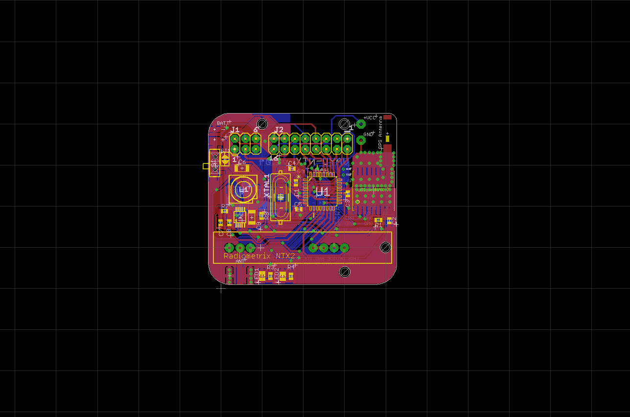
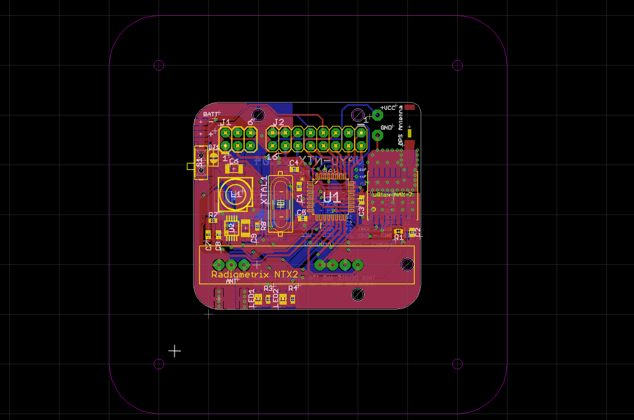
VAYU-NTX v1.04 with 10x10mm grid in Eagle.
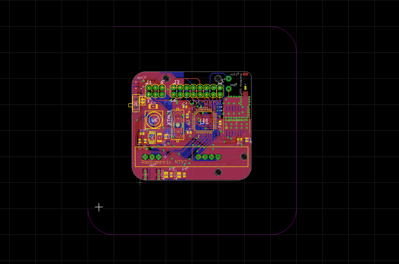
This can be done by either clicking on the dotted icon in the top left corner or going to VIEW – GRID. Set the size to 10, the unit to mm and set the Alt value to Finest by clicking on the Finest button. It doesn’t matter what units are set for Alt. I had previously aligned three of the holes on the VAYU-NTX PCB to be on a 10x10mm grid so it was an easy job to select everything with the group tool and move the group whilst holding Alt so that the holes aligned with the grid. After getting it as close as possible, I clicked on each hole individually whilst holding the CTRL key. This aligns them exactly to the grid. If your PCB hasn’t already got 2.5mm holes aligned to the 10x10mm grid, you will need to modify your design to comply. The pegs that are supplied with the pegboard are 2.5mm so set this size in Eagle and place your holes where the lines cross. It’s best to keep the holes on the outer edge to minimise the solder that gets on the pegs. Of course, if you can afford the extra PCB size, you could lay an extra border around it to accommodate the holes.
The next step is to create a new layer for your stencil outline. Click on the layer icon on in the tool bar on the left or click VIEW-Display/hide layers. You can then click NEW in the dialog and create your new Stencil layer.
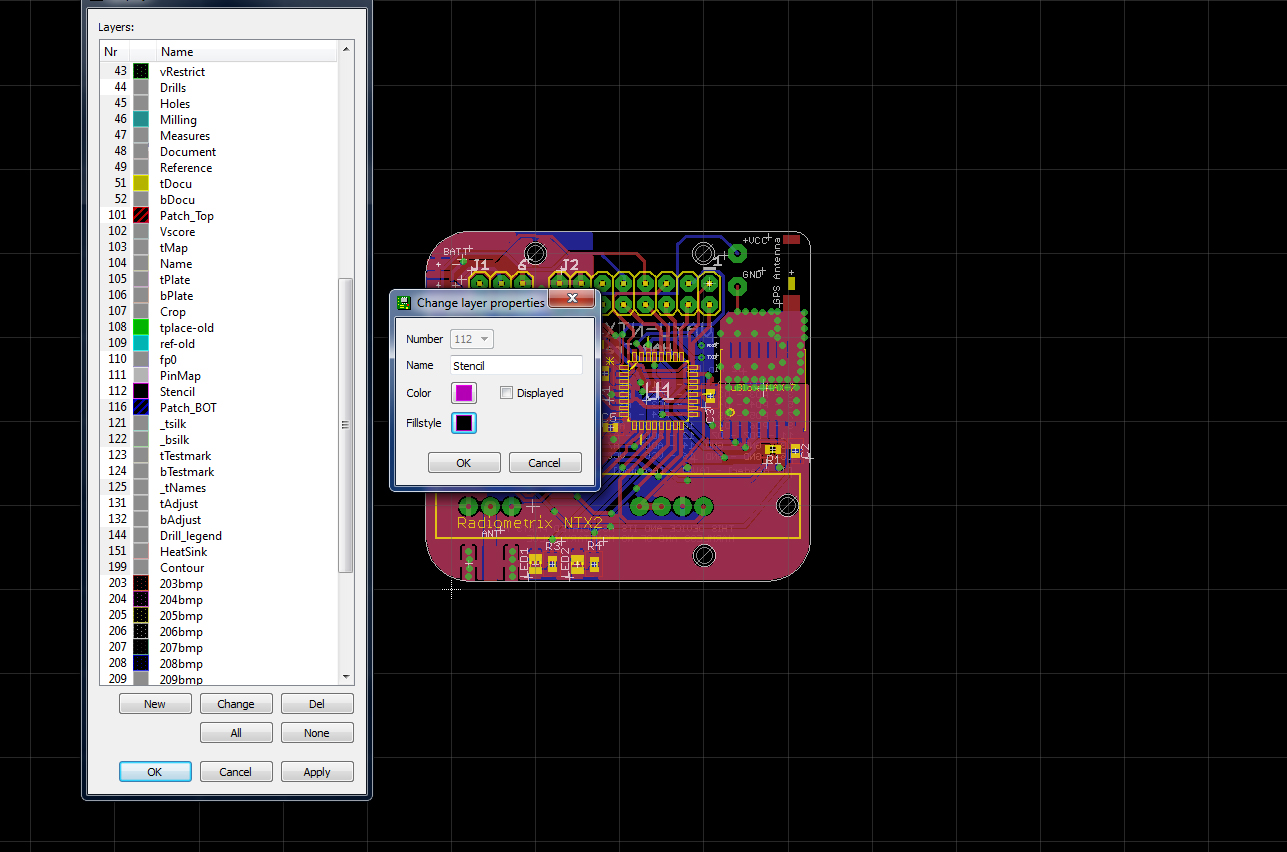
Creating a Stencil Layer in Eagle
I chose the name ‘Stencil’, the colour of Magenta to show up against the black background and the first fillstyle. Click on OK and again, OK and then on the wire icon. You can also click DRAW-WIRE. Before you draw, set the miter to 5mm in the toolbar and the width to 0. You can then draw a rounded rectangle or in my case, a square to represent the outline of the stencil. In our conversation, Mitch said he normally gives 30mm border around a PCB. For this example, I used roughly 20mm border for each side.
Drawing the Stencil Border on the new layer.
If you find it difficult to draw with the miter, set it to 0 and draw your shape with square sides. You can then set the miter to 5mm and click on each corner to make it rounded after the fact.
We now need to add the registration holes so that the solder stencil will lay immediately above the PCB. First, set the grid to .5mm. Then select the Circle tool and draw a 2.5mm circle with 0 width over the drill holes that are aligned with the grid.
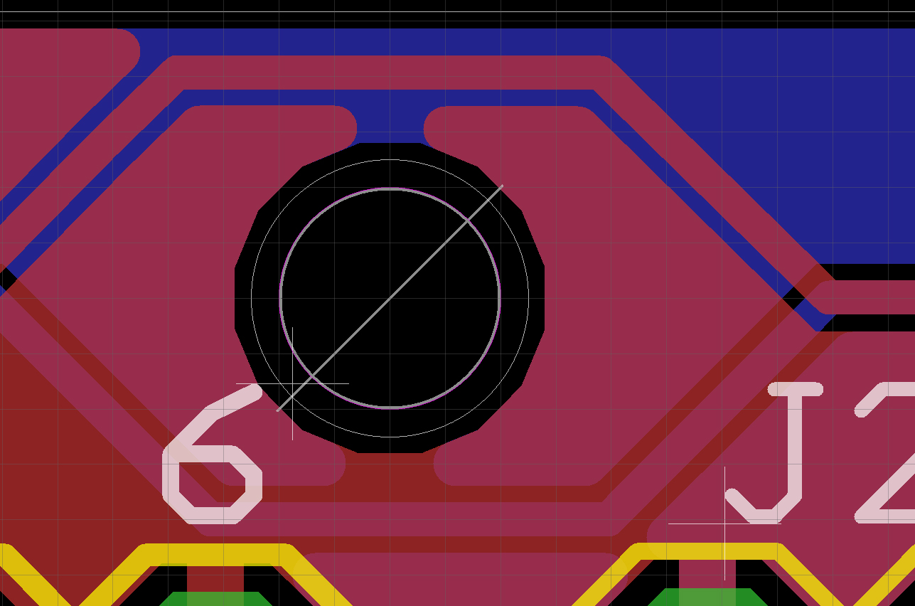
Drawing the new holes
Here I have zoomed the image up and you can just see the magenta outline of the new shape. To make it exactly 2.5mm, start the circle in the center of the drill hole and drag downward to it’s lower edge. Align it with the bolder inside circle of the drill graphic. Once you have successfully created one shape, duplicate it as many times as needed and lay the duplicates over the holes you require.

Duplicating the hole shape
In the above image, you can see the duplicated shape. Use your middle mouse button to pan to the next hole. You then need to duplicate some more hole shapes and place them on the border of the stencil. This is easily done in the same way.
All new hole shapes placed
Note that I have placed the holes on the nearest grid position to the edge of the stencil outline.
Now what’s required is to output a gerber file for the stencil. To do this, click on the CAM icon in the toolbar or click FILE-CAM Processor. Because I use Hackvana for my PCB fabrication, I had their CAM file already loaded. This makes no difference and you can start from a blank file.
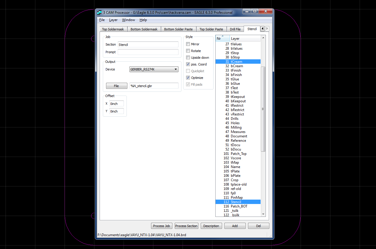
Setting the CAM file
I have named a new section to ‘Stencil’ since I intended to save the CAM Job after use. To create a new section, click on ADD and scroll to the right most section if not immediately visible. Set the device for GERBER_RS274X. Set the filename to %N_stencil.gbr This will use your projects filename and append ‘_stencil.gbr’ to it. Make sure pos. Coord and Optmize are checked. Then go into the layer list and make sure that only tCream and Stencil are highlighted. Then click on ‘Process Section’ and the gerber file will be created. You may see a yes/no dialog pop up regarding a drill file. If so, click on yes. I have not as yet found out what this means but it doesn’t seem to have a detrimental effect on the gerber files.
Next, you will need a program called Gerbv. Load the newly created gerberfile by clicking on FILE-Open Layer(s).

New file viewed in Gerbv
Using this program has two benefits. It allows you to check if your new stencil gerber file looks correct and affords very basic editing. In the above image, you can see me removing two pads by selecting them with a marquee (click’n’drag) and then pressing delete. You can individually click and delete shapes too. I edited these pads out because they are for the power supply and won’t necessarily be soldered up when the components are laid on the PCB. Once your edits are complete, you can FILE-EXPORT-RS-274(gerber) to save your completed stencil file.
Supply this file with your regular gerbers and you can order your Stencil along with your PCBs.